Campus Users
Trained Users—Each Session
New Users
Other Service Requests
External Users
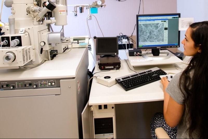
Get Started
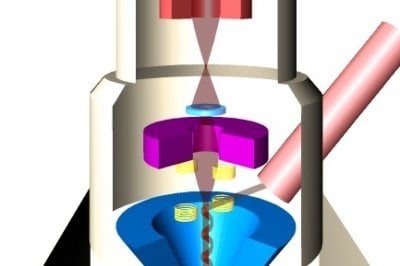
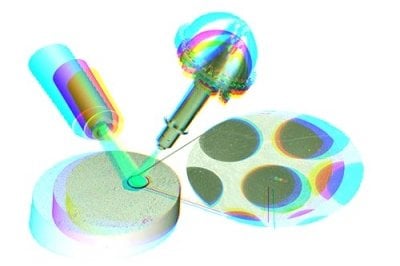
Request Analysis
Michigan Technological University and ACMAL have a history of collaborating with external clients, including for-profit, academic, and nonprofit organizations.